


Magazine Archive
Home -> Magazines -> Issues -> Articles in this issue -> View
The Transpozer (Part 2) | |
Article from Electronics & Music Maker, January 1983 | |
Part 2 completes this unique project unit with details of the LED Pitch Ratio Display
![]()
★ Pitch transpose ±1 octave
★ Pitch ratio display option
★ Delay and freeze facilities
★ External control input
★ Rack mounting case
This month we continue our exciting new project with detailed descriptions of the circuitry for the main unit and the Pitch Ratio display option along with practical uses for the unit.
COMPLETE KIT £160 excluding display option.
![]()
Figure 1. Circuit diagram of the Transpozer.
(Click image for higher resolution version)
Circuit Description
Figure 1 shows the complete circuit. The input amplifier stage IC1a allows the input sensitivity to be varied between microphone levels and synthesiser-type levels, using the level control RV1, and presents a high impedance to the input source. IC1c and d constitute the anti-aliasing filter, which is of the Sallen and Key equal capacitor value 4th order type with a Butterworth response, giving a 24dB/octave roll-off. The signal is monitored at this point by the comparator IC2a which drives the peak indicating LED, D4, when the signal level is beyond the converting range of the system. TR1 and IC12 together with C10 form the write sample and hold which presents sampled analogue levels to the conversion comparator IC8. Analogue levels converted back from digital data in the memory are sampled by TR2 onto C11. The signal is reconstituted by the sixth order Sallen and Key filter IC3b, c and d, giving a roll-off of 36dB/octave. The mix control RV2 then mixes the treated signal from the re-constituting filter with the 'dry' signal from the input amplifier to produce a composite signal at the wiper of RV2 which then passes to the output. R1 ensures high frequency stability even with highly capacitive loads. Some of the treated signal, controlled by the feedback control RV3, may be mixed with the 'dry' signal by IC1b for subsequent re-processing.
IC13a provides a control voltage for the read clock in accordance with the settings of the pitch shift controls, RV4 and RV5, and the voltage on the external control voltage input, J3. IC13b via SW3 allows an offset to be applied to IC13a to give additional flexibility in choice of external control voltages. The write clock, IC2c and d, sets the timing for the conversion processes. In the harmony mode SW1a is open leaving C20 to bring about a 40kHz write clock frequency. In the delay mode, with SW1 closed, the parallel combination of C20 and C21 lowers the clock frequency to about 20kHz. The write clock output is passed to the storage area via IC20 and is returned, slightly delayed, to the conversion section. The timing of the conversion process is clarified by the timing diagram shown in Figure 2. Analogue to digital conversion is initialised when the write clock goes low, causing IC4 pin3 to go high. On the next high to low transition of the 600kHz HF clock IC4a the flip-flop IC5b is set. A short pulse is gated from the high signal now on IC5 pin 9 by the monostable formed by IC6c and IC4c. This pulse is used to start the SAR, IC7. As explained previously, the digital word is built up in the SAR bit by bit. The first bit, however, is a polarity bit which is set up by IC8 before the IC5a flip-flop changes the mode of the DAC, IC9, from its decode mode to its encode mode. The remainder of the bits are set up with IC5a set and thus with IC9 in its encode mode. IC8 compares the input voltage with the IC9 encode output current derived from data being put on the data bus by the tri-state buffers IC10 and 11.
Figure 2. Logic timing diagram.
The two current output ports from IC9 each have two connections although they are not differential outputs; only one is used at a time, depending on the polarity of the signal. R18, 19 and R21, 22 must therefore be of close tolerance to keep the signal symmetrical and hence keep the distortion low. The output of IC8 determines the bit state at each approximation. The last bit to be determined is the least significant bit. When all bits have been set up the data remains on the data bus and is written into memory until the write clock goes high, at which time the flip-flops IC5a and b are reset and the tri-state buffers are disabled. The data bus is then loaded with data read from the memory and IC9, now in its decode mode, converts this data directly into an analogue current on its decode outputs, pins 16 and 17, and subsequently to a voltage at IC3 pin 1. IC2 pin 1 goes high at this time allowing the converted voltage to be sampled by TR2 for re-constitution by IC3b, c and d. TR1 is also gated to take a sample of the input voltage at the same time, ready for the next analogue to digital conversion. The sampled voltage is not held frozen until the write clock goes low once again.
Now referring to the storage section, the read clock IC14 has a frequency range of about 20kHz to 80kHz, determined by a +/-10V control voltage on pin 5. The read clock increments the read address counter, IC15, which is a CMOS binary ripple counter. The number of memory location addresses and hence the delay time is determined by the count at which IC15 is reset to zero, and is set by SW2a. The write address counter, IC16, is clocked similarly by the write clock from IC2d. The two addresses set up by the two counters are selected by means of the multiplexer, IC17, 18 and 19, under the control of the write clock signal on IC20 pin 6. The selected address is then put on the memory address bus. When SW1b is open the multiplexer is forced into the write address select mode to enable reading and writing to occur at the same address when in the delay mode. Since four 8-bit memory IC's are used the relevant section is selected by means of the decimal decoder, IC21, giving the storage IC's 22 to 29 the requisite chip select signals, depending on the states of A9 and A10. Data is written to and read from the memory on the data bus.
The memory write signal on IC20 pin 8 has a delayed falling edge caused by R68 and C29 to give the address counters, the multiplexer and the store address lines plenty of time to settle down before the store IC's are put into the write mode. Random memory locations would otherwise become corrupted as the address bits change state. When the freeze, or repeat, footswitch at J4 is closed the memory IC's are locked in the read mode, preventing any change in the contents of the store.
![]()
Figure 3. Circuit diagram of the Power Supply.
(Click image for higher resolution version)
The power supply circuit, shown in Figure 3, is quite conventional, using IC regulators to provide the three DC voltages. The purpose of R69 is to reduce power dissipation by IC31. The analogue and digital ground rails are kept separate on the PCB, even though they are eventually connected at the 0V input. This helps to keep at bay any logic switching noise which could otherwise find its way into the audio input.
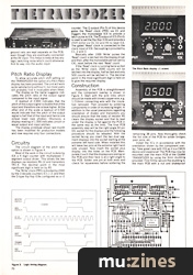
The Pitch Ratio display ±1 octave.
Pitch Ratio Display
To allow accurate pitch shift setting on the TRANSPOZER the option of a Pitch Ratio display has been provided. The unit will work quite satisfactorily without it, but most users will probably find it invaluable when fitted.
The display as the name suggests indicates the pitch ratio of the output signal compared to the input signal.
A readout of 2.000 indicates that the pitch of the output signal is double that of the input and therefore one octave higher. At the other end of the scale a readout of 0.500 would indicate that the pitch of the output signal is half that of the input and hence one octave lower (see photos). Obviously, a display reading of 1.000 indicates unison or equal output and input pitches.
The display prototype shown last month has been modified for production models and now requires only four connections.
![]()
Figure 4. Circuit diagram of the Pitch Ratio display.
(Click image for higher resolution version)
Circuitry
The circuit diagram of the pitch ratio option is shown in Figure 4.
Most of the work in the circuit is done by IC6 a 4 digit counter with multiplexed 7-segment output driver. This drives the two displays via resistors R6-12 and transistors TR1-4. The decimal point in the most significant digit is held on by R5.
The 'Write' clock (PR5) is divided by 2000 by the 3 decade counters IC's 1-3, and then the D-type flip-flop IC4a configured as a +2 counter. The Q output (Pin 5) of this device gates the 'Read' clock (PR4) via D1 and triggers the monostable IC5 to provide a latch pulse to IC6. The 0 output of IC5 (Pin 6) is used to set the flip-flop IC4b and provide a short pulse via C6, D2 and R4 to reset IC6. The gated 'Read' clock is connected to the clock input of IC6. Decoupling is provided by C1, 2 and 3.
Basically after 1000 'Write' pulses the 'Read' count is latched into the display driver and then, after the monostable period (set by C4), reset before the next 'Read' count.
If the 'Read' clock is running twice as fast as the 'Write' clock, 2000 counts will be latched into the display, half as fast and only 500 counts will be latched in. The decimal point in the most significant digit is held on to give the required display.
Construction
Assembly of the PCB is straightforward and the component overlay is shown in Figure 5. Start with the wire links which should be made with tinned copper wire, e.g. 1/0.6mm connecting wire with the insulation removed. Then proceed by soldering components in order of increasing height. In addition to the usual precautions regarding orientation of diodes and transistors you should ensure that the body of resistor R5 clears the display socket and that its lead under the display is flat against the PCB in the same way as the links. The final PCB assembly step will be the right angle 40 pin DIL socket for the displays and the following procedure should be adopted. With the socket facing you insert the two dual segment displays into the socket starting at the extreme left hand side. When installed this will leave two pins at the extreme right hand side unused. Now insert the socket plus display into the holes on the PCB. Manipulate it such that the displays are resting on the PCB and their face is at a right angle to the PCB. Solder one pin at both ends and check for squareness before soldering the remaining 38 pins. Now thoroughly check the foil side of the PCB for solder bridges, poor joins, etc.
![]()
Figure 5. Component overlay of the display PCB.
(Click image for higher resolution version)
Install the IC's in accordance with the orientation shown by the component overlay. Take great care with IC6 as it is a CMOS device and expensive! The PCB may now be mounted over the main PCB of the E&MM TRANSPOZER by using the 3mm studding provided. First firmly secure the studding to the main PCB with a nut and shakeproof washer on either side of the PCB. Place nuts on each of the pillars so formed and locate them about 1 to 2 cms from the top. The pitch ratio indicator PCB is now located onto these pillars. The unit is lined up with the cut-out for the display and the nuts on the pillars adjusted such that the PCB is resting upon them and is parallel with the main PCB. The display should be firmly in the panel cutout and if not then remove the PCB and while holding the base of the pillars gently bend them forward. There is sufficient spring in the studding to provide a secure mounting once the displays are lodged in the panel cut-out. Next secure the PCB to the pillars with nuts and shakeproof washers.
The final step, which is to be carried out after the main PCB has been checked, is to connect four wires from the 'Veropins' PR1, PR2, PR4 and PR5 on the display PCB to the 'Veropins' on the main PCB having the same identification - refer to TRANSPOZER component overlay, Figure 2 given last month. Note that the prototype pitch ratio indicator also required a -12V supply which was available from PR3 on the main TRANSPOZER PCB. This connection is no longer required. 1/0.6mm insulated wire is used for the connecting wires and these connections are to be kept short such that they do not droop over components on the main PCB. For the 0V line (PR1) the wire should be shaped so that it runs at the same height as the display PCB and then drops down at the rear of the main PCB and along the back edge to PR1.
No adjustments are required and the pitch ratio indicator may be checked as follows. Switch power on and observe that the +5V LED is illuminated. Check the +5V supply at pin PR2 to ensure that its level has not been affected. With the E&MM TRANSPOZER in the 'harmony' mode turn the wide pitch control and observe that the indicator changes from about 0.500 to 2.000 for full rotation. The display PCB has a generously sized cut-out which allows easy access to RV7 and RV8 for the calibration step.
The display board mounted on the main board.
Using the Unit
The controls are quite self explanatory. The sensitivity control is adjusted so that the peak LED just flickers on the loudest passages. This setting will achieve the best possible dynamic range. The input amplifier sensitivity can be adjusted to allow a high impedance microphone to be used. The other end of the sensitivity range allows electronic sources such as synthesisers to be directly injected. The output of the TRANSPOZER remains constant at about 500mV, so no matter what input source you use, the output should be connected to the high level input of your amplifier or tape recorder.
With the mode switch in the delay position, no pitch shifting occurs, allowing all the common delay related effects to be obtained with a delay time dependant on the setting of the delay select switch over the range 6mS to 200mS. The shift controls are obviously ineffective in the delay mode. The mix control being used to adjust the contrast and delayed signals. The feedback control allows the delayed signal to be re-circulated to produce echo effects at long delay settings through reverb effects at medium delays to constant flanging effects at short delay settings. The repeat facility is most useful in the delay mode since longer passages can be captured. Delay setting 6 achieves the most useful results. To repeat a passage, the footswitch is operated just after the passage has been played or sung, and held for as long as the repeated passage is required. While the passage is repeating, playing can continue to accompany it, the mix control being used to adjust the contract between the repeated and direct signals.
In the shift mode, the Coarse shift control sets the interval in the range ±1 octave. The Fine shift control gives very precise pitch trim adjustment of ±½ semitone. The delay time switch now controls the shifted passage length. Longer delays produce smoother sounding shifts, but at the expense of introducing unavoidable ADT effects when shifting up, and missing notes when shifting down. In most applications, delay setting 5 will achieve the most satisfactory results. The feedback control now allows some very interesting effects to be produced. For instance, if the shift control is set to 3 semitones up, and feedback is used, then the shifted pitch will re-circulate producing harmonies of 3 semitones up plus 6 semitones up plus 9 semitones up etc, resulting in chord-like sounds. The repeat facility can be used in the shift mode, albeit with a reduced passage length. Only the shifted part will be repeated, allowing the dry signal to be played along with the repeating harmony. A signal, once frozen by the repeat footswitch can be shifted with a different interval to the shift setting used during capture, allowing some very unusual variable speed and pitch percussive sounds to be produced.
Some particularly fascinating effects are produced when the shift interval is very close to unison. With plenty of feedback, each recycled shift will be fractionally higher (or lower for downward shifts) resulting in gradually rising (or falling) notes after they have been played. With slightly less feedback and delay 3 and 4 selected, cyclic flanging is produced. With just a little feedback, the mix control central and delay 4 selected, beautiful chorus effects are produced. This is particularly effective on a 6 string guitar, producing some very convincing 12 string sounds. The chorus effect can also "beef-up" the sound of a single VCO synthesiser, giving multiple VCO sounds.
The CV input could be used along with an external pre-set voltage switching network to enable rapid selection and changes of shift interval to be achieved. Alternatively, if a low frequency sinewave oscillator is connected to the CV input, true vibrato can be produced.
Since the shift controls are continuous, Table 1 provides a list of semitone intervals and required pitch ratios, allowing precise musical intervals to be set.
The completed Display Board.
Although the E&MM TRANSPOZER was designed with economy in mind, the specifications have been kept very reasonable. The only limitations to be aware of are firstly that of the cyclic glitching that is produced in the shift mode each time a fresh passage of the input is selected for treatment. Some very elegant electronic "splicing" techniques have been used in some of the more expensive commercial units to overcome the problem, frequently employing a microprocessor to handle the very complex signal "juggling" algorithms. No glitching noise reduction has been designed into the E&MM TRANSPOZER due to the high cost of even a partial solution. The problem should not be too limiting in most applications, particularly with careful selection of the delay time, and subtle use of the mix control. The problem is more noticeable at higher feedback levels, which should be avoided in the shift mode. The other possible limitation is that of the quantisation noise that is only just noticeable on instruments such as bass guitars that have very little high frequency content. This is very simply overcome by turning down the amplifier treble control. However, the quantisation noise is hardly noticeable on most sound sources.
Most musicians will gladly accept these slight disadvantages considering the many effects offered by this versatile and comparatively inexpensive unit.
PARTS LIST FOR PITCH RATIO INDICATOR
| Resistors, 1/4W 5% carbon film | ||
| R1,2 | 1k0 | 2 off |
| R3,4 | 4k7 | 2 off |
| R5 | 150R | |
| R6,7,8.9,10,11,12 | 56R | 7 off |
Capacitors | ||
| C1,2,3 | 100n ceramic disc | 3 off |
| C4,6 | 22n polyester | 2 off |
| C5 | 100p polycarbonate | |
Semiconductors | ||
| IC 1,2,3 | 74LS90 | 3 off |
| IC4 | 74LS74 | |
| IC5 | 74LS122 | |
| IC6 | 74C925 | |
| TR1,2,3,4 | BC182L | 4 off |
| D1,2 | 1N4148 | 2 off |
| DIS 1,2 | CQX87A or equiv. | 2 off |
Miscellaneous | ||
| 14 pin DIL sockets | 5 off | |
| 16 pin DIL socket | ||
| 40 pm right angle DIL socket | ||
| Veropins | 4 off | |
| Mounting hardware and connecting wire | ||
| PCB |
Table 1. Interval Settings
| Shift Up | Shift Down | ||
| Semitones | Ratio | Semitones | Ratio |
| 12 | 2.000 | -1 | 0.944 |
| 11 | 1.888 | -2 | 0.891 |
| 10 | 1.782 | -3 | 0.841 |
| 9 | 1.682 | -4 | 0.794 |
| 8 | 1.587 | -5 | 0.749 |
| 7 | 1.498 | -6 | 0.707 |
| 6 | 1.414 | -7 | 0.668 |
| 5 | 1.335 | -8 | 0.630 |
| 4 | 1.260 | -9 | 0.595 |
| 3 | 1.189 | -10 | 0.561 |
| 2 | 1.122 | -11 | 0.530 |
| 1 | 1.059 | -12 | 0.500 |
Specifications
| Max Delay Time | almost 200mS |
| Pitch Shift Range | +1 octave |
| CV Input Range | 0 to +5V |
| Dynamic Range | 72dB |
| Frequency Response | |
| Treated signal | 8Hz to 8kHz — 6dB |
| Dry Signal | 8Hz to 34kHz — 3dB (maximum gain) |
| Input Sensitivity | 5mV to 500mV rms |
| Output Level | 500mV rms |
A complete kit for parts for the Transpozer including the case, front panel, PCB and all components is available from E&MM, (Contact Details) at £159.95 including postage, packing and VAT. Please order as Transpozer kit.
The Pitch Ratio Display board kit is also available at £32.95 including postage, packing and VAT. Please order as Transpozer Display Kit.
These units are supplied with the co-operation of Digisound Ltd.
Overseas customers please add £10 for carriage.
Series - "Transpozer"
This is the last part in this series. The first article in this series is:
The Transpozer
(EMM Dec 82)
All parts in this series:
Part 1 | Part 2 (Viewing)
More with this topic
 The Spectrum Synthesiser - Professional Quality Monophonic Instrument (Part 1) |
 Workbench - STAGE LIGHTING INTERFACE BOARDS |
 Putting on the Style |
 An Ultra VCO From The 4720 |
 Studio Earthing Techniques - Interconnect (Part 1) |
 Eliminating Patch Cords Without Eliminating Capability - A Practical Approach |
 The Layman's Guide to Digital Logic Gates - (in one easy lesson) |
 Voice Frequency to Voltage Converter |
 Multi-waveform LFO |
 Lab Notes: The Polyphonic Synthesizer |
 The RackPack |
 Technically Speaking |
Browse by Topic:
Electronics / Build
Publisher: Electronics & Music Maker - Music Maker Publications (UK), Future Publishing.
The current copyright owner/s of this content may differ from the originally published copyright notice.
More details on copyright ownership...

Electronics & Music Maker - Jan 1983
Feature by Paul Williams
Previous article in this issue:
Next article in this issue:
Help Support The Things You Love
mu:zines is the result of thousands of hours of effort, and will require many thousands more going forward to reach our goals of getting all this content online.
If you value this resource, you can support this project - it really helps!
Donations for June 2026
Issues donated this month: 0
New issues that have been donated or scanned for us this month.
Funds donated this month: £0.00
All donations and support are gratefully appreciated - thank you.
Magazines Needed - Can You Help?
Do you have any of these magazine issues?
If so, and you can donate, lend or scan them to help complete our archive, please get in touch via the Contribute page - thanks!